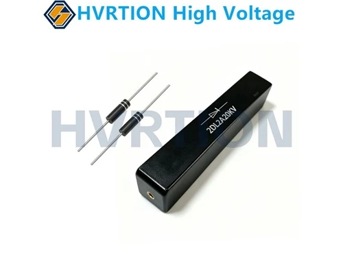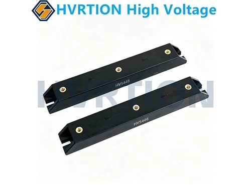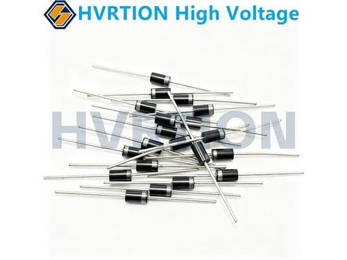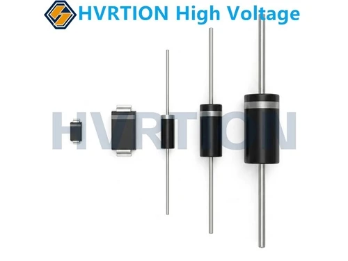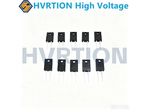
Therefore, in chip design, optimization of Trr can be abandoned, and all efforts can be focused on increasing the effective chip area. A larger chip area means lower current density, more uniform heat distribution on the chip surface, and lower junction-to-case thermal resistance at the same rated current. Taking the CL01-12 series power frequency high-voltage diode as an example, at a 12kV withstand voltage and a 350mA rated current, the typical VF is approximately 12V, and the conduction power dissipation is approximately 4.2W.
However, for the same withstand voltage rating, the fast recovery version, in order to reduce Trr to below 100ns through doping recombination centers, may have a VF that rises to 15V or even higher, resulting in a power dissipation difference of nearly 30% at the same 350mA. For an industrial dust collector power supply running 16 hours a day, 365 days a year, this 30% power dissipation difference accumulates to a significant amount in electricity costs. Under the same rated current, the chip area of the power frequency version is usually 30% to 50% larger than that of the fast recovery version. This is the fundamental reason why it can carry the same current with a lower VF - larger area, lower current density, and more complete conductance modulation effect.